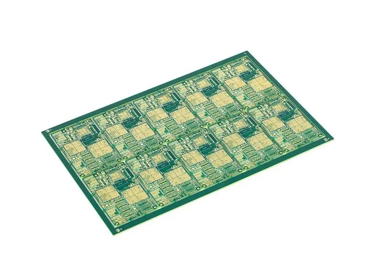
Q: What are HDI (High-Density Interconnect) circuit boards and how are they manufactured?
A:
Q: What defines HDI circuit boards?
A: HDI circuit boards are multilayered circuit boards created using stacked layers and micro-via technology. Essentially, they are constructed by first obtaining a core board, typically with or without plated through-holes (PTH) using traditional methods, and then adding stacked layers with fine lines and micro-vias on both surfaces to form a multilayered circuit board.
Q: How are micro-vias defined in the context of PCB (HDI circuit boards)?
A: Micro-vias are typically defined as holes with a diameter smaller than 150 micrometers (6 mil) within the PCB (HDI circuit boards). These holes are too small to be achieved using conventional mechanical drilling methods.
Q: What characterizes buried holes in the context of HDI circuit boards?
A: Buried holes, known as Buriedholes, are holes embedded within inner layers that are not visible in the final product. Compared to through-holes, their advantage lies in not occupying surface area, allowing more components to be placed on the PCB (HDI circuit boards). Buried holes are typically mechanical holes with a diameter of 0.2mm or more.
Q: How are blind holes defined in the context of HDI circuit boards?
A: Blind holes, known as Blindholes in HDI circuit boards, are visible in the final product but can only be seen on one side, unlike through-holes that are visible on both sides. The advantage of blind holes over through-holes is that beneath the blind hole location, wiring can be placed. Mechanical blind holes are usually achieved using mechanical drilling to control depth, while laser blind holes are obtained through laser technology.
Q: How is the quality of HDI circuit boards ensured through various testing methods?
A:
Q1: What is the focus of the solderability test for HDI circuit boards and which standards are followed?
A: The solderability test mainly examines solder pads and electroplated vias following standards like IPC-S-804. Tests include edge dip, rotation dip, wave dip, and solder ball tests.
Q2: How are internal defects in HDI boards detected, and which methods are employed?
A: Microsection analysis using techniques outlined in standards like IPC-TM-650 is typically used for detecting internal defects. This includes measuring copper and solder alloy plating thickness, alignment of internal conductor layers, delamination, and copper cracks.
Q3: What aspects are assessed in HDI board size and visual inspections, and what specialized equipment is used?
A: Size inspection covers hole diameter, spacing, tolerances, and edge dimensions. Visual defect inspection includes alignment of solder mask to pads, impurities, delamination, wrinkles in solder mask, alignment of circuit patterns, layer separation, etc. Dedicated equipment comprising a computer, automatic workstation, and imaging systems is often used for this purpose.
Q4: How is the integrity of the solder mask on HDI boards tested, and what are the challenges faced with certain types of solder masks?
A: Dry film solder masks and optical imaging solder masks are commonly used on HDI boards. Challenges with dry film masks, including detachment and fragility, are addressed through strict thermal stress testing during incoming inspection. Observing detachment after stress testing or immersing boards in water or cleaning agents helps identify potential defects due to stress, fragility, or chemical damage.
Q: What issues does the production of HDI (High-Density Interconnect) circuit boards aim to address?
A:
1. Why is uniform plating thickness crucial for HDI circuit boards?
Uniform plating ensures consistent quality and reliable performance across the board, especially for complex circuitry and miniaturized components.
2. How does optimizing equipment and current density improve output?
Optimizing these factors enhances productivity, allowing for higher yields within the manufacturing process.
3. What’s the significance of controlling the copper substrate within a 1-5μM range using optimized plating solutions?
Maintaining this specific range ensures precise control over the copper substrate, crucial for HDI board functionality.
4. Why is it essential for the plating solution to possess good dispersion properties for the board’s micro and through-holes?
Effective dispersion aids in uniform plating and reliable connectivity across intricate micro and through-holes.
5. Why is minimizing recesses within the same plating solution critical for HDI board production?
Reducing recesses ensures consistency in plating thickness, especially crucial for the functionality and reliability of HDI boards.
6. How do issues like severe contamination of the copper surface and plating solution affect HDI board production?
Severe contamination affects the cleanliness and quality of the plating, leading to potential defects and reliability issues in the final product.
7. What standards are necessary for plating on thin base copper sheets using high current density?
Maintaining uniformity in plating thickness and quality on thin base copper sheets demands specific standards to ensure reliability and performance.
To address these challenges, what features does the developed horizontal electroplating production line possess?
The horizontal electroplating production line adopts a segmented distribution approach rather than using insoluble phosphor copper anodes as the standard. This distribution method involves installing rectifiers with varying power in different plating segments to provide diverse current densities, ensuring uniform thickness for the plating on thin base copper. The rectifier system must offer stable direct current or pulsing for electroplating. Pulse plating, compared to traditional direct current, enhances coating purity, reduces porosity, and improves coating uniformity. Pulse plating is a type of modulated current electroplating, essentially operating as an on-off switch for direct current, but in millisecond-level cycles.
Q: What are the differences between the processes of browning and blackening in HDI circuit board manufacturing?
A:
Q: How do browning and blackening contribute to HDI circuit board production?
A: Both browning and blackening processes aim to enhance the bonding between the copper foil and the resin in HDI circuit boards. Poor browning can lead to issues like oxidation and incomplete etching in the inner layers, causing problems like inadequate plating.
Q: What are the specific roles of browning in the HDI circuit board process?
A:
Removing surface contaminants: Browning eliminates grease and impurities, ensuring surface cleanliness.
Time-sensitive compression post-browning: It’s crucial to compress the boards within a specific timeframe post-browning to prevent water absorption and potential board delamination.
Creating a uniform fuzz layer: Browning creates an even fuzz layer on the copper surface, enhancing the bond between the substrate and the resin to prevent delamination.
Q: What similarities exist between browning and blackening in HDI circuit board manufacturing?
A: Both processes aim to:
A. Increase contact area between copper foil and resin: Enhancing the bonding between these components.
B. Improve resin wetting on copper surfaces: Facilitating resin flow into corners for stronger adhesion post-curing.
C. Generate a fine passivation layer on the copper surface: Preventing reactions between hardening agents and copper under high-temperature, high-pressure conditions to avoid delamination.
Q: What are the key differences between browning and blackening in HDI circuit board manufacturing?
A:
Thickness of fuzz layer: Blackening and browning result in different thicknesses of the fuzz layer.
Control complexity: Blackening solutions are more challenging to control compared to browning solutions.
Cost: Blackening solutions tend to be more expensive than browning solutions.
Micro-etching rates: Blackening solutions induce a higher micro-etching rate compared to browning solutions.
Quality implications: Blackened surfaces may exhibit greater roughness; slight scratches or repairs in inner layer traces might be better concealed by blackening compared to browning.
Hope our above answers can help you, if you are looking for some high-quality PCB manufacturers, you can visit here:eashub.com